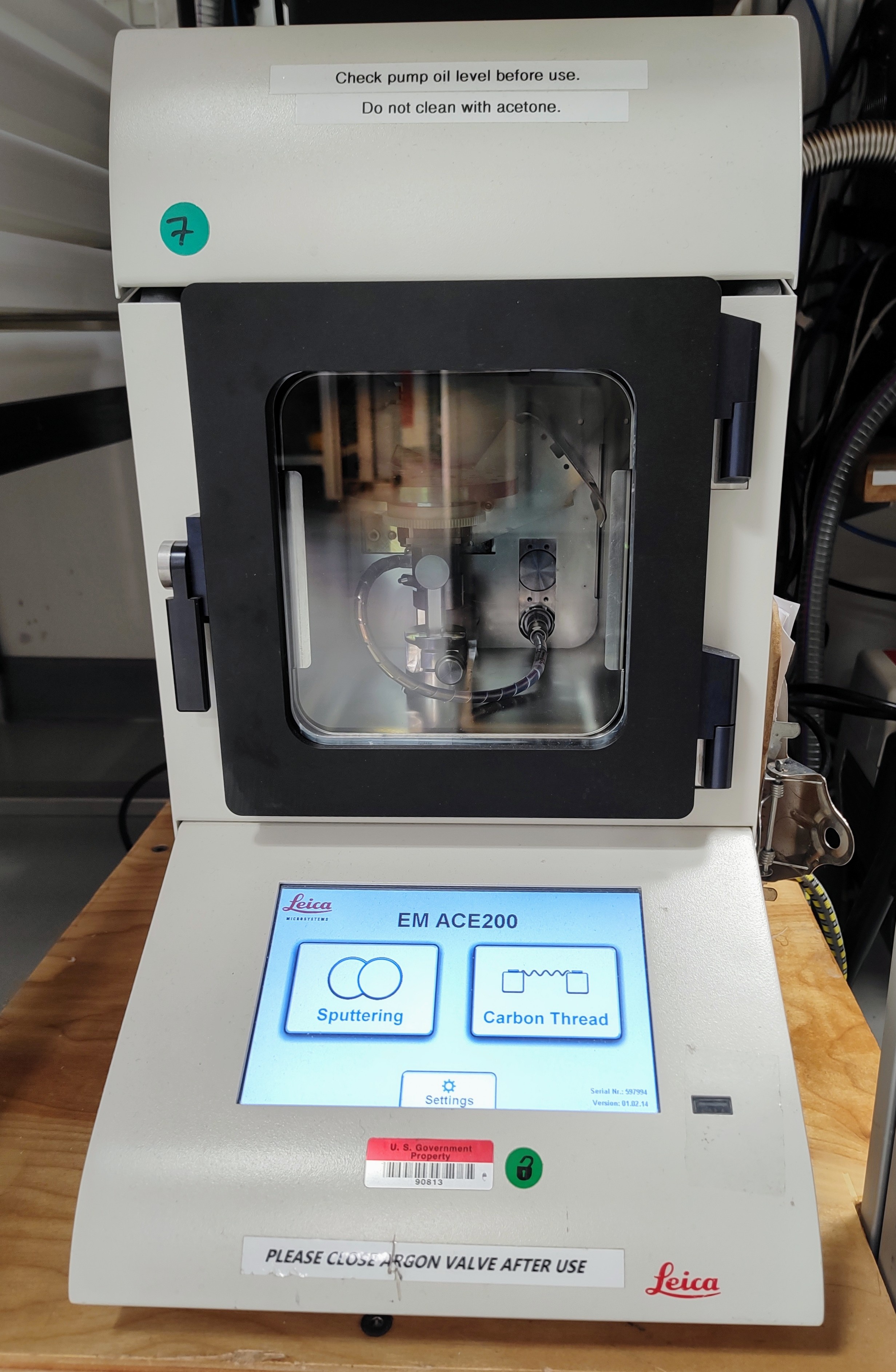
The Leica EM ACE200 (Image from Leica: https://www.leica-microsystems.com/products/sample-preparation-for-electron-microscopy/p/leica-em-ace200/)
Introduction
Sputter coating in scanning electron microscopy (SEM) is the process of covering a specimen with a thin layer of conducting material; either a metal, such as a gold/palladium (Au/Pd) alloy, or carbon (C). A conductive coating is needed to prevent charging the specimen with an electron beam in the SEM high-voltage mode.
While metal coatings are also useful for increasing signal-to-noise ratio, they are of inferior quality when energy-dispersive X-ray spectroscopy (EDS) is employed. For this reason, when using EDS a carbon coating is preferred.
With the Hitachi TM3000 SEM, sputter coating is not required for all samples. Images up to a magnification of ×4000 are of high quality without any sputter coating when operating in the Charge-up Reduction Mode (Settings > Observation Mode).
For detailed observations in magnifications greater than ×4000 and very delicate fossils, sputter coating before using the SEM can be used to potentially obtain higher quality images.
Apparatus and Material
The sputter coater on the JOIDES Resolution is a Leica EM ACE200 that supports carbon coating and Au/Pd sputtering. Other metal targets are supported as well; however, we are using only the Au/Pd system at this time.
The following quick introduction should give an overview of the different coating options and the resulting layer of conductive material. The sample material for this test is sand. The following coating options were selected as shown in Tables 1 and 2.
Material: Gold-Palladium | |||||
|---|---|---|---|---|---|
Specimen No. | Rotation speed | Coating direction | Coating time(sec) | Purge cycles | Coating time(min) |
1 | 1 | Directional | 15 | 2 | 7 |
2 | 1 | Directional | 25 | 2 | 10 |
3 | 1 | Diffuse | 30 | 2 | 7 |
4 | 1 | Directional | 25 | 5 | 9 |
5 | 1 | Diffuse | 30 | 5 | 7 |
Table 1. Au/Pd coating settings.
Material: Carbon | |||
|---|---|---|---|
Specimen No. | Threading | Pulse/flash | Coating time (min) |
6 | Single | 1 pulse | 3 |
7 | Single | 5 pulses | 3 |
8 | Single | 2 flashes | 3 |
Table 2. Carbon coating settings.
The venting process after each sputter coating process takes 99 sec.
Figure 1 shows the coated stubs. The stub in the upper left corner was not sputtered, numbers 1–8 were sputtered with gold-palladium and/or carbon. The sputtering parameters are listed above in Tables 1 and 2.
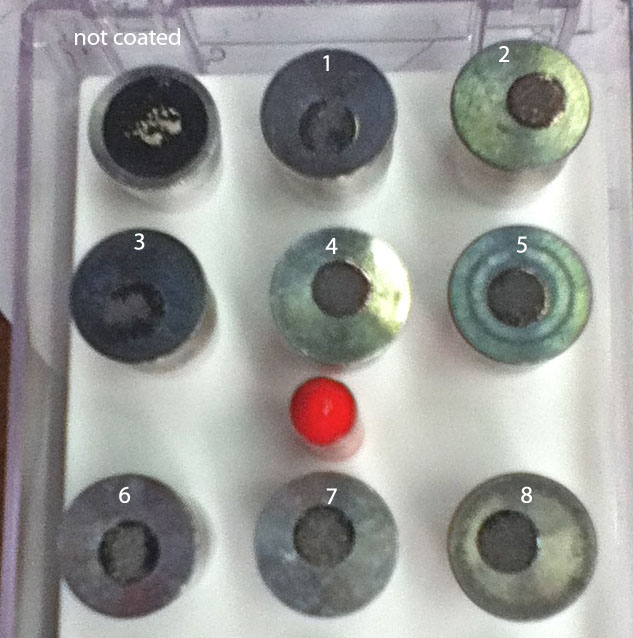
Figure 1. Coated Stubs.
Each stub was checked for image quality using the Hitachi SEM TM3000, as shown in Figure 2.
No. 1, x200 | No. 1, x1000 |
|
|
No. 2, x200 | No. 2, x1000 |
|
|
No. 3, x200 | No. 3, x1000 |
|
|
No. 4, x200 | No. 4, x1000 |
|
|
No. 5, x200 | No. 5, x1000 |
|
|
No. 6, x200 | No. 6, x1000 |
| |
No. 7, x200 | No. 7, x1000 |
|
|
No. 8, x200 | No. 8, x1000 |
|
|
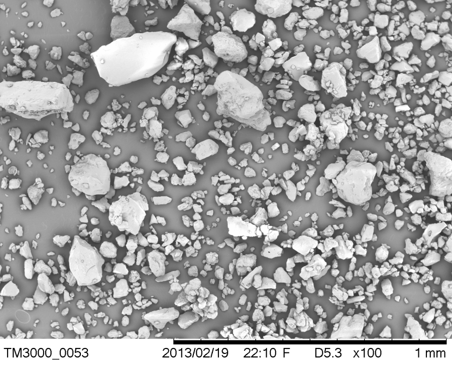
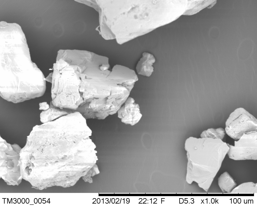
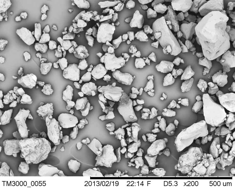
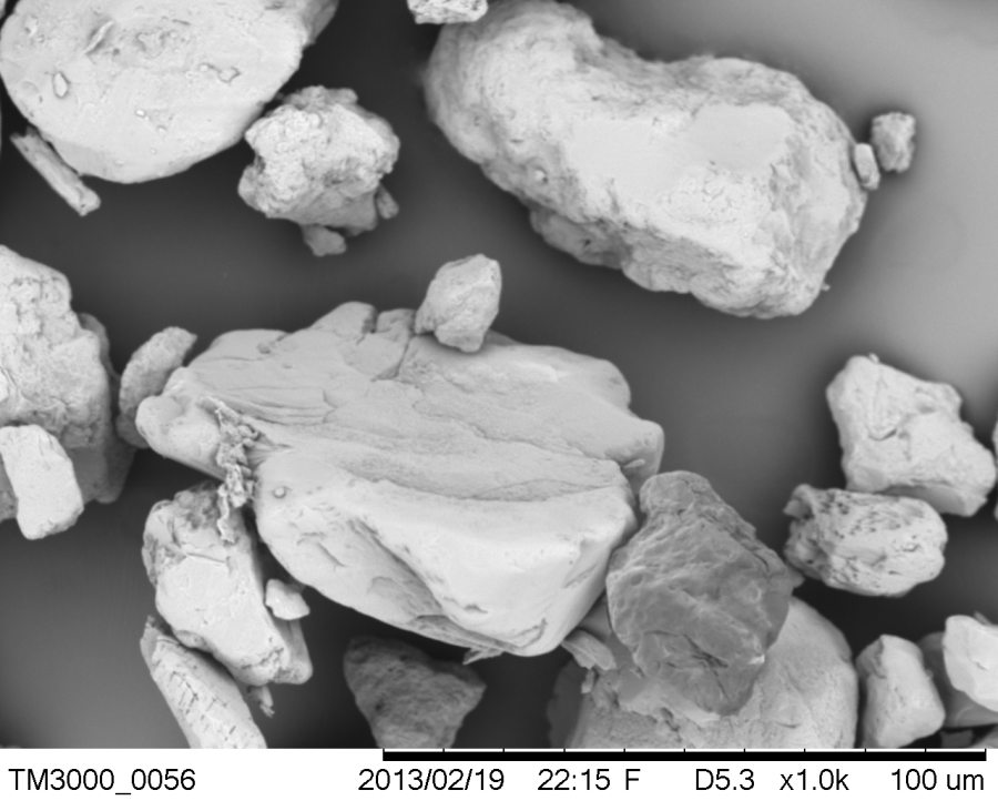
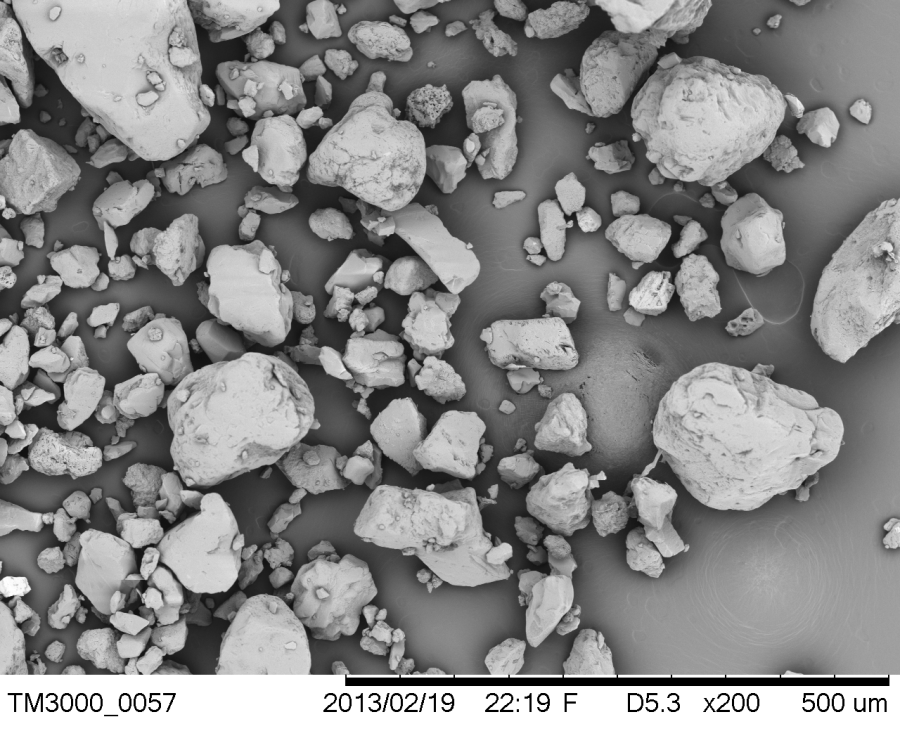
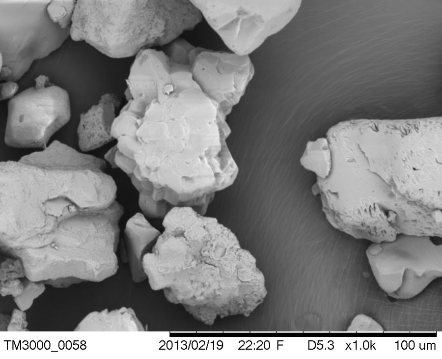
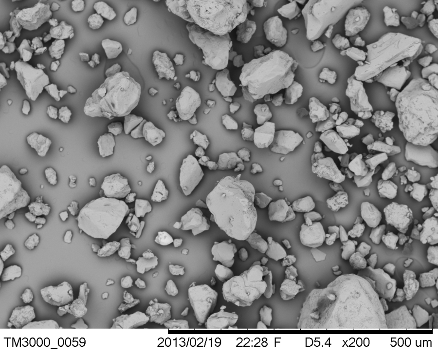
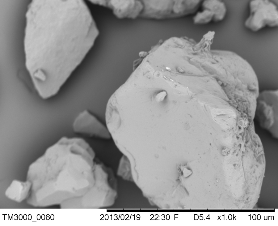
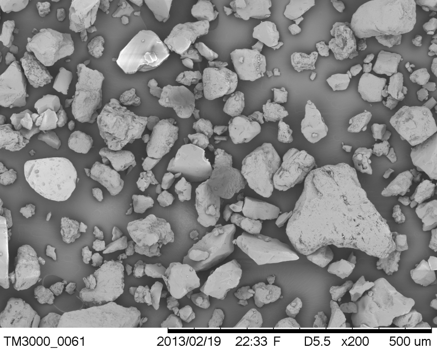
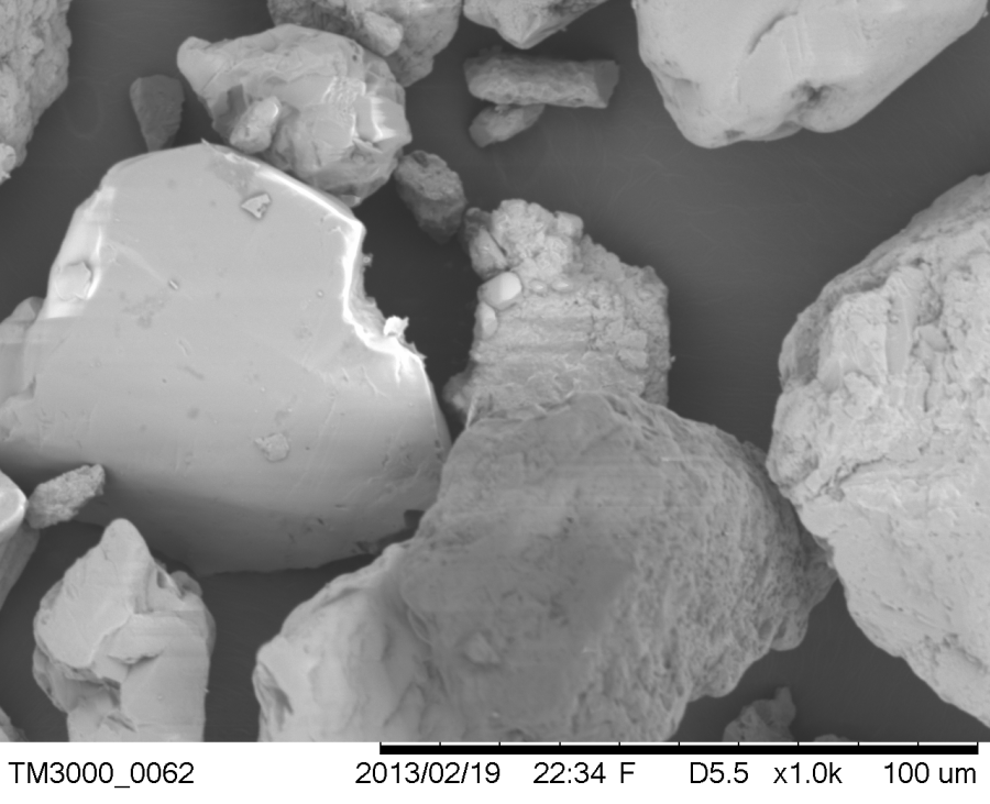
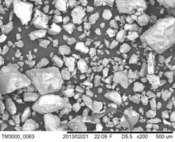
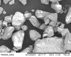
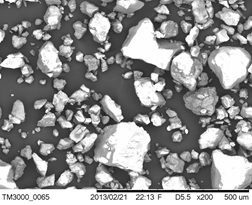
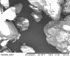
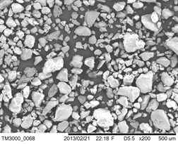
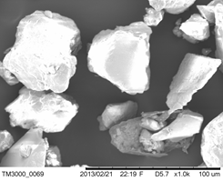
Figure 2. SEM Images of Coatings.
Observations
- Sputter coating with gold-palladium results in a more evenly distributed thin layer compared to carbon thread sputtering.
- When sputtering with metal, purge cycles of >2 provide a better distribution of the metal.
- A sputter duration between 25 and 30 sec gives the best results in metal distribution and thus provides the best images.
Recommended settings
- For Au/Pd coating, the following settings are recommended:
- Sputter duration: 25-30 seconds
- Purge cycles: >2
- For C coating, the following settings are recommended:
- Double carbon thread
- Pulse mode
- 15 pulses
Credits
This document originated from Word document Coating/Sputtering Differences on SEM Stubs: User Guide.docx (see Archived Versions below for a pdf copy) that was written by S. Herrmann in 2013 and edited during Expedition 374 by A. DeLoach. Credits for subsequent changes to this document are given in the page history.
1 Comment
Unknown User (25dbb4e563432e130164eb687464000b)
Aug 08, 2018Reviewed Agust 8, 2018.